In the first part of this post, I will combine the generate keyword with a for loop to implement a PISO using D flipflops. In fact, in an earlier post, I have done it using individual D flipflop instantiations. You can refer to that code from here, PISO in Gate level and Behavioral level Modeling.
PISO using Generate & for keywords:
--library declaration.
library ieee;
use ieee.std_logic_1164.all;

--parallel in serial out shift register
entity piso is
port(Clk : in std_logic;  --Clock signal
    parallel_in : in std_logic_vector(3 downto 0);  --4 bit parallel load
    load : in std_logic;  --active high for loading the register
    serial_out : out std_logic  --output bit.
    );
end piso;

architecture gate_level of piso is

signal D,Q : std_logic_vector(3 downto 0) := "0000";

begin

serial_out <= Q(3);

--entity instantiation of the D flipflop using "generate".
F :  --label name
    for i in 0 to 3 generate   --D FF is instantiated 4 times.
    begin  --"begin" statement for "generate"
    ----usual port mapping. Entity instantiation with named association
        FDRSE_inst : entity work.FDRSE1 port map
            (Clk => Clk,
            ce => '1',
            reset => '0',
            D => D(i),
            set => '0',
            Q => Q(i));
    end generate F;  --end "generate" block.
--The D inputs of the flip flops are controlled with the load input.
--Two AND gates with a OR gate is used for this.
D(0) <= parallel_in(3) and load;
D(1) <= (parallel_in(2) and load) or (Q(0) and not(load));
D(2) <= (parallel_in(1) and load) or (Q(1) and not(load));
D(3) <= (parallel_in(0) and load) or (Q(2) and not(load));

end gate_level;
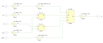
The FDRSE flip code can be copied from here: Synchronous D Flip-Flop with Testbench.
I believe that the code is self explanatory. The for loop is used to instantiate as many number of modules as we want to instantiate. To easily port map in a programmatic way, I declare a std_logic_vector for D and Q, and use the index "i" to connect bits of the individual signals to the ports of the individual flipflops.
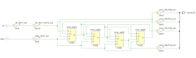
Johnson Counter using Generate Statement:
Next I want to show you how to combine generate statement with both if else conditional statement and for loop, to programmatically instantiate multiple components. For this I will be using the example of a Johnson counter.
library ieee;
use ieee.std_logic_1164.all;

entity johnson_counter is
port(clk : in std_logic;
    reset : in std_logic;
    count : out std_logic_vector(3 downto 0)
    );
end johnson_counter;

architecture Behavioral of johnson_counter is

signal D,Q : std_logic_vector(3 downto 0):="0000";
signal not_Q4 : std_logic:='0';

begin

--Q of the last flipflop is fed to the D of the first flop
not_Q4 <= not Q(3);
count <= Q;  --Q is assigned to output port

--generate the instantiation statements for the 4 fliflops
--F,F0 and F1 are label names for the generate statement.
--'generate' statements should have a 'begin' and an 'end'
F : for i in 0 to 3 generate
    begin
        F0 : if (i = 0) generate  --instantiate the "first" FF only.
            begin U1 : entity work.FDRSE1 port map --usual port mapping
                (Clk => Clk,
                ce => '1',
                reset => reset,
                D => not_Q4,
                set => '0',
                Q => Q(0));
            end generate F0;
        F1 : if (i > 0) generate --generating the rest of the three FF's.
            begin U2 : entity work.FDRSE1 port map   --usual port mapping
                (Clk => Clk,
                ce => '1',
                reset => reset,
                D => Q(i-1),
                set => '0',
                Q => Q(i));
            end generate F1;
    end generate F;

end Behavioral;
You can get the testbench for the Johnson counter from this post: 4 bit Johnson Counter with Testbench.
The FDRSE flip code can be copied from here: Synchronous D Flip-Flop with Testbench.
As you can see from these examples, using "generate" keyword makes your code much more smaller and neat. They even help others to go through and understand your code faster.
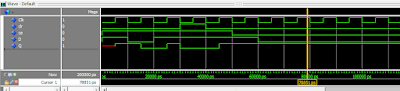
Make sure to visit the older posts linked in the above post to get the testbenches and see screenshots of the simulation waveform.